Indian Scientists Develop Indigenous Normally OFF High Electron Mobility Transistor
- Posted By
10Pointer
- Categories
Science & Technology
- Published
20th Mar, 2021
-
Context
- Indian scientists have developed a highly reliable, High Electron Mobility Transistor (HEMTs) which are required in power electronics applications.
What is High-Electron-Mobility Transistor (HEMT)?
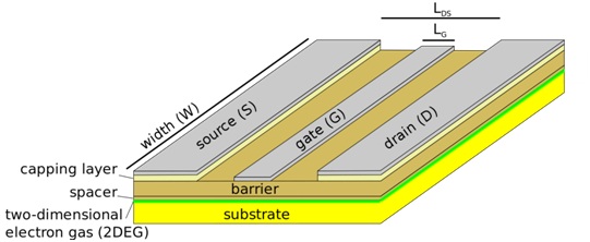
- A high-electron-mobility transistor (HEMT), also known as heterostructure FET (HFET) or modulation-doped FET (MODFET).
- It is a field-effect transistor incorporating a junction between two materials with different bandgaps as the channel instead of a doped region.
- A commonly used material combination is GaAs with AlGaAs.
- Since GaAs has higher electron affinity, free electrons in the AlGaAs layer are transferred to the undopedGaAs layer where they form a two-dimensional high mobility electron gas within (10 nm) of the interface.

Applications
- These are similar to those of MESFETs – microwave and millimetre wave communications, imaging, radar, and radio astronomy – any application where high gain and low noise at high frequencies are required.
- Gallium nitride HEMTs on silicon substrates are used as power switching transistors for voltage converter applications.
|
About the developed High Electron Mobility Transistor (HEMTs)
- The HEMT is a normally OFF device.
- It can switch currents up to 4 Ampere and operates at 600 Volts.
- This first-ever indigenous HEMT device is made from gallium nitride (GaN).
- Application: It is useful in electric cars, locomotives, power transmission and other areas requiring high voltage and high-frequency switching.
- Specific transistors called HEMTs made of aluminium gallium nitride/ gallium nitride (AlGaN/GaN) provides an edge over silicon-based transistors as they allow the systems to operate at very high voltages, switch ON and OFF faster, and occupy less space.
- The developed technology is a first of its kind, which uses a type of chemical called ternary oxide (composed of two different metal ions combined in an oxide matrix or Al, Ti and O), which behaves like material having a larger positive charge concentration (p-type material).
- Significance:It does away with intrinsic reliability and performance issues of the in-use industrial techniques for e-mode HEMTs, allowing the development of efficient power switching systems.
- This device will now be taken up for the prototype development and field-testing level.
- With a growing market for electric vehicles in India, such an indigenous development can make India self-reliant for transistor technology, the statement said.